Sponsors: Analog Devices, NSF POETS Center, SRC
Students: Heungdong Kwon, Dr. Joe Katz, Dr. Aditya Sood, Dr. Marc Dunham
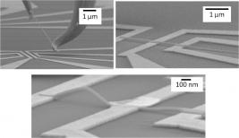
The most innovative energy conversion technologies, ranging from solar and thermoelectrics to lasers (which convert electric energy to light), are benefitting from nanostructures and/or nanostructured materials. Thermal phenomena play a central role in the performance and reliability of devices based on these technologies, and we are collaborating with multiple groups on the characterization of these devices as well as on the related transport physics and properties.
Recent progress has focussed on nanolayers of MoS2 and related VDW multilayers, into which ion migration can be used to store energy and (as an important biproduct) modulate the thermal conductivity. Our activities in this area have included practical thermoelectric conversion structures, based on silicon, for application in low-grade heat recovery. Thermal engineering of these coverters needs a detailed and careful handling of packaging in order to achieve significant impact. We’ve also worked on quantum well laser nanostructures, in which electron confinement enables efficient optical devices in silicon for compatibility with conventional IC circuits. Power absorption in these nanostructures strongly degrades their power emission capabilities and motivates our recent measurements of thermal and optical properties. Additional work is focused on the thermal and thermoelectric properties of nanowires and nanowire films.
Given the multidisciplinary nature of this project, the collaborations span many departments and types of companies and are often student-initiated and led by group members.